SAMSUNG

SAMSUNG

  • search
  • menu

Clean Tech Innovation

We collaborate with
an open mind and support communities,
startups and suppliers.

As an industry leader,

We fully acknowledge and embrace the impact and
responsibility associated with our brand.

We aim to do our part in supporting clean tech innovations
by investing in promising technologies and developing our
own initiatives.

We are collaborating with international universities
and research institutes to solve environmental problems and are
exploring and investing in promising eco-conscious
technologies and projects for the future.

Leading the way
in clean tech
innovation

How Samsung
Electronics is working
towards
clean tech innovation

Research in carbon capture and clean air technologies
Application of carbon capture
technology to semiconductor manufacturing facilities after 2030
Utilization of technology to detect
and analyze particulate matter in
local communities by 2030
Development of proprietary clean air technology Learn more
Tackling environmental
challenges
Active discovery of and investment in promising clean technologies
and environment-related startups
through internal and external venture support program
Learn more

Research in Carbon
Capture
and Clean Air
Technologies

We are committed to helping address environmental challenges.

From reducing carbon
emissions to capturing
emitted carbon to use as a
new resource

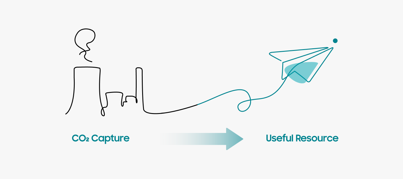
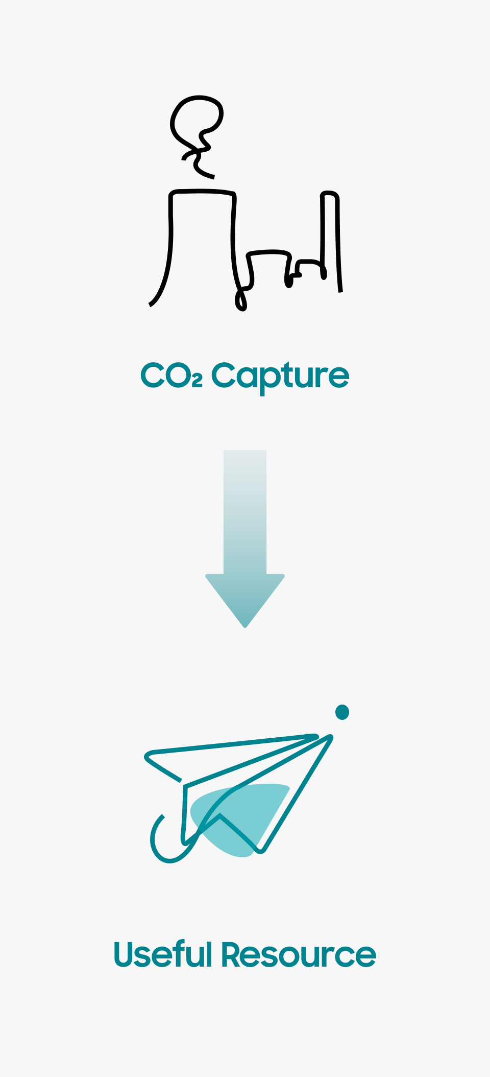
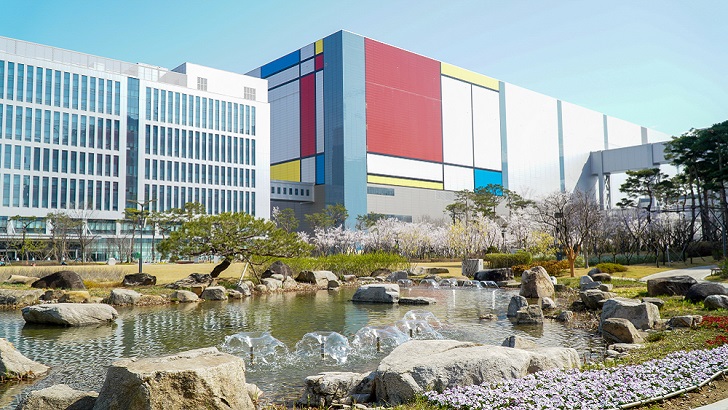
We established the Carbon Capture Research Institute (now restructured as Air Science Research Center) to develop and commercialize carbon capture and utilization technologies that store carbon emitted from semiconductor manufacturing sites and recycle it as a resource.

In September 2021, the institute was founded with the aim of developing technology that efficiently collects greenhouse gases with less energy, converting them into useful resources, and promoting cooperative research with domestic and international universities and research institutes.

We aim to apply and expand carbon capture technology in our semiconductor manufacturing facilities after 2030.

We are also working on recycling process CO₂, purifying high-concentration CO₂ emissions from semiconductor manufacturing, and repurposing it as a CO₂ resource for our material use.

With the goal of reducing 50,000 tonnes of CO₂ emissions per year by 2030, we aim to recycle post-use CO₂ into new CO₂ needed for semiconductor manufacturing, thereby reducing Scope 1 and 3 emissions.

Process gas reduction
technology

DS Division operates gas treatment and processing facilities, assessing gas decomposition characteristics, emissions volume, and overall energy efficiency.
The RCS (Regenerative Catalytic System) mainly treats gases emitted from the etching process in a large-capacity, energy-efficient treatment facility.
We apply a POU (Point Of Use) to each production facility’s emissions during the CVD (Chemical Vapor Deposition) process to reduce emitted gases.

Carbon Capture & Utilization

CO2 Capture Useful Resource CO2 Capture Useful Resource

Research areas and
objectives (applicable
candidate technology)

  • Membrane gas
    separation
  • Catalyst and
    plasma
  • Direct
    electrochemical
    conversion
  • Bio
    Tech

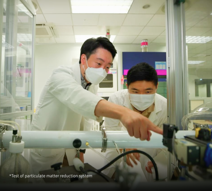
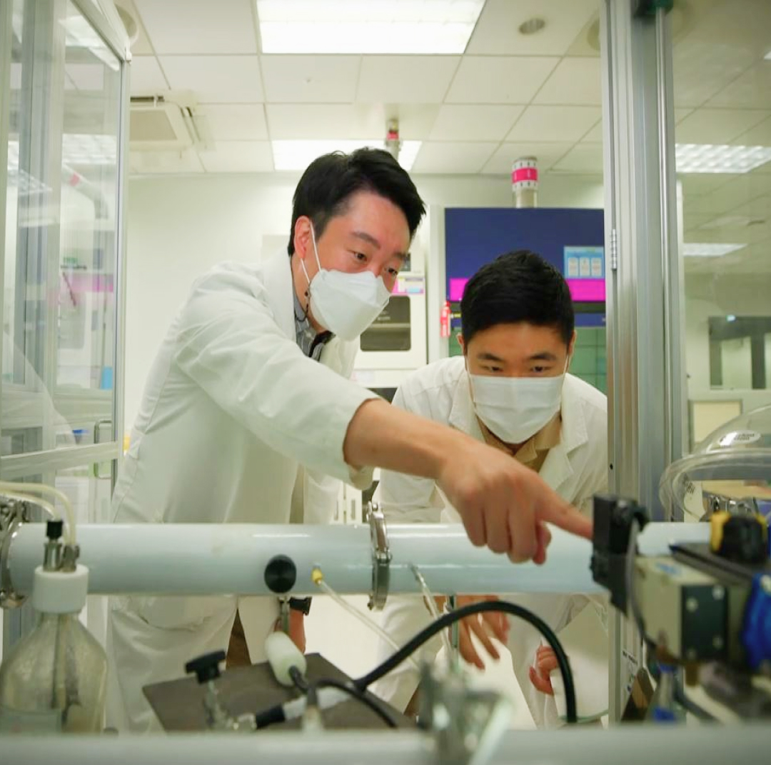
Reducing particulate
matter to improve
the quality of air
we breathe

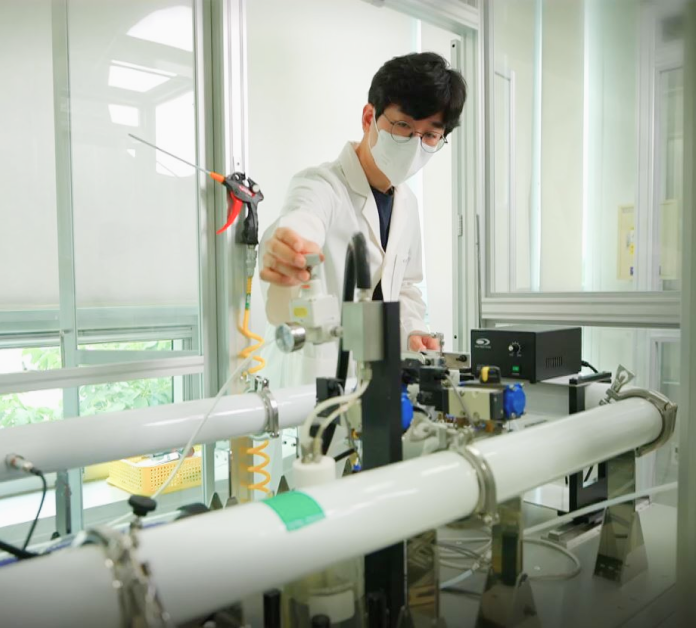
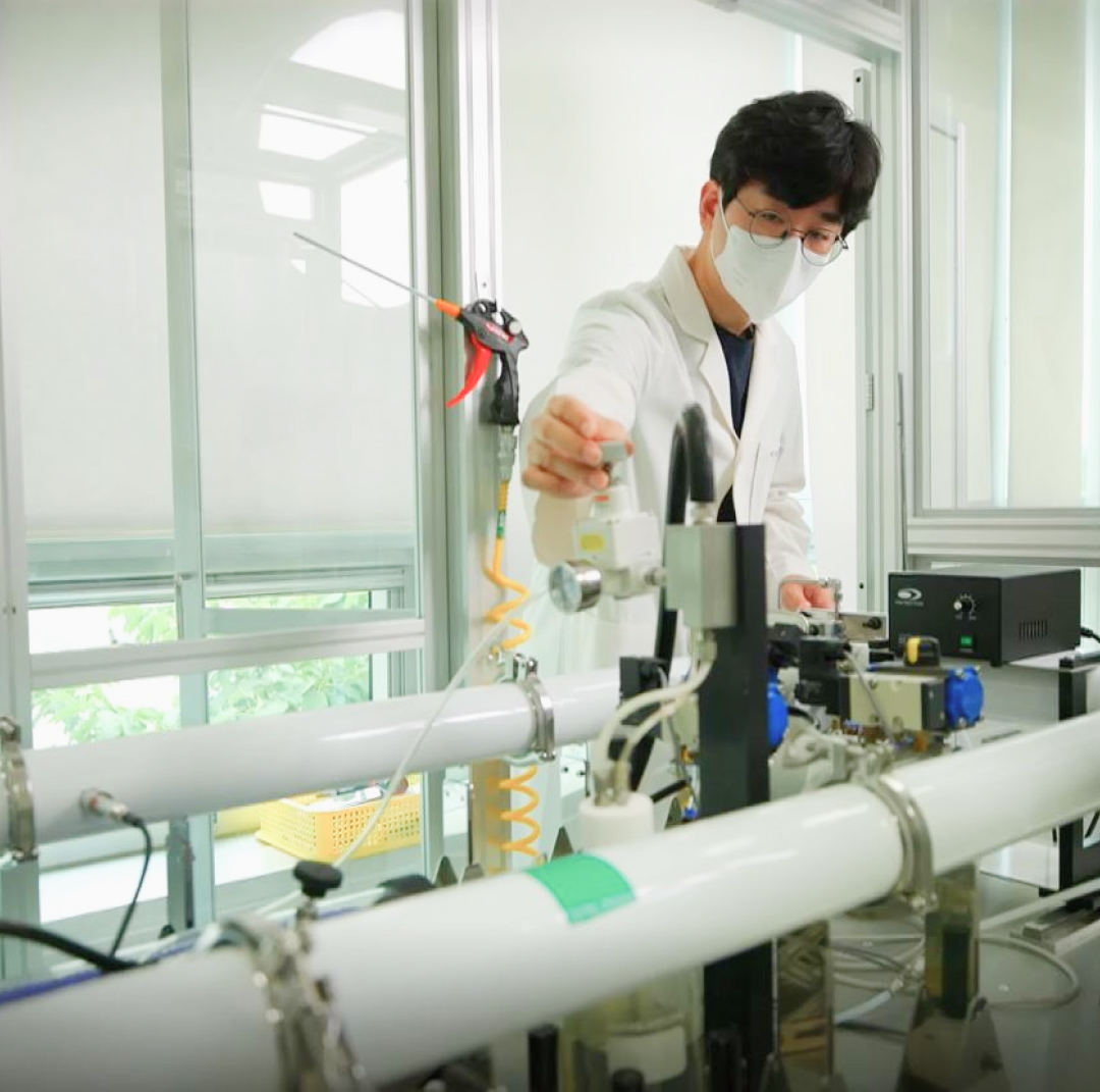
We established the Air Science Research Center (previously Particulate Matter Research Institute) in January 2019, dedicated to developing innovative filters and original technologies to detect, analyze, and remove particulate matter.

We successfully developed air purification filter capable of removing both fine particles and gases, which can be easily cleaned with water and reused for up to 20 years. We are piloting a prototype using this technology in air-conditioning facilities like bus terminals, underground parking lots, and DS Division buildings, as well as in test rooms and partner company offices. From 2030, we aim to expand the application of this prototype.

Ongoing proprietary
technology research in
particulate matter
reduction

  • Analyzing the root cause of air pollution

  • Diagnosing particulate matter and
    causative gases

  • Creating sensors, catalysts and system technology for particulate matter
    reduction
  • *Test of particulate matter reduction system *Test of particulate matter reduction system
*Test of particulate
matter reduction
system

Tackling
Environmental
Challenges

Shape the future
with innovative technology

C-Lab supports
innovative ideas for a
sustainable future,
in-house and externally

We operate the C-Lab, a program that discovers and supports the development of creative ideas –including those relating to sustainability – inside and outside of Samsung Electronics.

In addition to discovering promising future technologies, we find and support in-house ventures and startups, which seek to solve environmental challenges.

C-Lab

Discovering and
expanding investment
in
innovative startups
in Sustainability areas

Investment fields

  • Technologies related to high efficiency, low energy
    consumption, and sustainable materials and parts
  • Technologies related to net zero carbon emissions,
    renewable energy and resource circularity

Supporting our partner
companies in their
journey towards net
zero
and investment in
environmental
resources through
Samsung Electronics'
ESG Fund

  • Field of support
    Technologies related to net zero carbon emissions,
    renewable energy and circular resources
  • Operation plan
    Funds for facilities related to carbon
    reduction or environmental safety

    Technological developments
    Funds for operations

Digital Library

  • Environment Safety Policy
    for Workplace

News & Story